- Applications
- Emulation and Prototyping
- Emulation and Enterprise Prototyping
Emulation and Enterprise Prototyping
Breakthrough performance and integration for ASIC and SoC emulation
Hardware emulation is the process of debugging and functionally verifying a system early in the development phase. Emulation requires quick turnaround time when processing design changes as well as high design accessibility and debug visibility to improve ASIC designer productivity.
Emulation and prototyping methodology and customer requirements have changed considerably in recent years. Enterprise prototyping is an emerging market that blends emulation with traditional prototyping to provide a solution with enhanced debuggability, high capacity and performance, and the ability to interact with a wide range of peripherals and stimulus.
To maximize system performance for emulation and enterprise prototyping platforms, AMD delivers the industry’s largest capacity adaptive SoC and FPGA1 with improved I/O and transceiver latency. The AMD Vivado™ ML design suite delivers a state-of-the-art development experience with new implementation features designed to improve compile time and QoR.
AMD offers significant advantages for developing emulation and enterprise prototyping platforms:
- Fast place-and-route to improve productivity for large ASIC and ASSP designs
- Full visibility debug solutions, including configuration-based readback, writeback, and state capture
- Re-entrant debug probe modifications for quick debug turnaround
- Reduced system-level power consumption
- High utilization and QoR supporting ASIC-like clocking and routing structures
Documentation
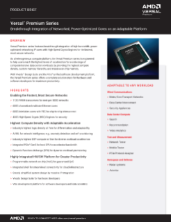
Breakthrough performance and integration for ASIC enterprise prototyping and emulation can be realized with the AMD Versal™ Premium VP1902 adaptive SoC. The VP1902 device doubles emulation and enterprise prototyping system platform performance with 2X the logic capacity2, reduced I/O and transceiver latency, and an enhanced two-by-two SLR array compared to the market leading Virtex™ UltraScale+™ VU19P device. Vivado™ ML edition enhanced place-and-route features simplify design and increase productivity by significantly reducing compile time and improving QoR. These silicon and tool enhancements together provide the ideal solution for tackling the demands of cutting-edge ASIC and SoC platforms.
World’s Highest Logic Capacity Adaptive SoC1
Reduces the number of partitions and simplifies board layout
Enables 2X larger platform capacity2
Enables 2X higher system performance3

Solution Summary and Benefits
- Vivado ML implementation tools
- Reduced compile time
- Improved QoR
- ASIC-like clocking efficiently maps complex ASIC and SoC clock trees
- High bandwidth and low-latency I/O and transceivers
- Efficient pin multiplexing between FPGAs
- Reduced latency across partitions for improved system performance
- Industry support with our High-Speed Transceiver Pin Multiplexing IP
- Debug Solutions
- Full debug visibility supporting configuration-based readback, writeback, and state capture
- High-speed debug over PCIe®
- Deep storage ILA to offload capture data to external memory
- Based on AMD internal analysis in May 2023 with a 6-input LUT count to compare the Versal Premium VP1902 device versus the Intel Stratix 10 GX 10M FPGA. (VER-002)
- Based on AMD internal analysis in May 2023, comparing the number of system logic cells of the Versal Premium VP1902 device versus the Virtex UltraScale+ VU19P device. (VER-001)
- Based on AMD internal system clock performance analysis in May 2023, comparing the Versal Premium VP1902 device to the Virtex UltraScale+ VU19P device across a range of design sizes and cut nets. (VER-006)
- Based on AMD internal analysis in May 2023, comparing the latency in nanoseconds of an AMD Versal adaptive SoC XPIO in an 8:1 mux configuration with bypass FIFO mode enabled to a Virtex UltraScale+ FPGA HP I/O with no bypass FIFO option. Actual results will vary. (VER-008)


