
Design Entry & Implementation
Overview
Vivado™ supports design entry in traditional HDL like VHDL and Verilog. It also supports a graphical user interface-based tool called the IP Integrator (IPI) that allows for a Plug-and-Play IP Integration Design Environment.
The Vivado ML Edition delivers the best-in-class synthesis and implementation for today’s complex FPGAs and SOCs with built-in capabilities for timing closure and methodology.
The UltraFast methodology report (report_methodology) that is available in the default flow of Vivado, helps users constrain their design, analyze results, and close timing.
Features
Here's a quick overview of Vivado™ Design Suite features for design entry and implementation. Click the other tabs for complete feature details.
IP Integrator
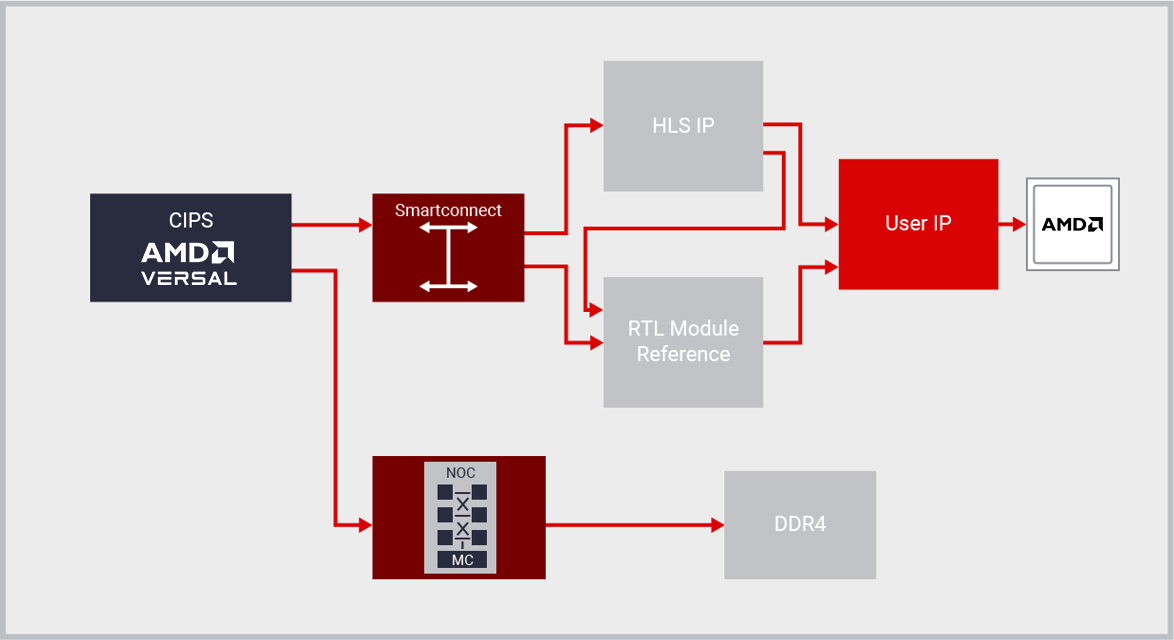
The Vivado™ ML Edition shatters the RTL design productivity plateau by providing the industry’s first plug-and-play IP integration design environment, with its IP Integrator feature.
Vivado IP Integrator provides a graphical and Tcl-based, correct-by-construction design development flow. It provides a device and platform aware, interactive environment that supports intelligent auto-connection of key IP interfaces, one-click IP subsystem generation, real-time DRCs, and interface change propagation, combined with a powerful debug capability.
Designers work at the “interface” and not “signal” level of abstraction when making connections between IP, greatly increasing productivity. Often times this is using industry standard AXI4 interfaces, but dozens of other interfaces are also supported by IP integrator.
Working at the interface level, design teams can rapidly assemble complex systems that leverages IP created with Vitis HLS, Model Composer, AMD SmartCore™ and LogiCORE™ IP, Alliance Member IP as well as your own IP. By leveraging the combination of Vivado IPI and HLS customers are saving up to 15X in development costs versus an RTL approach.

Vivado IP Integrator Key Features and Benefits
- Seamless inclusion of IP Integrator hierarchical subsystems into the overall design
- Rapid capture and packaging of IP Integrator designs for reuse
- Support for both graphical and Tcl-based design flows
- Rapid simulation and cross-probing between multiple design views
- Support for processor or processor-less designs
- Integration of algorithmic (Vitis HLS and Model Composer) and RTL-level IP
- Combination of DSP, video, analog, embedded, connectivity, and logic
- Support for Project based DFX Flow
- DRCs on complex interface level connections during design assembly
- Recognition and correction of common design errors
- Automatic IP parameter propagation to interconnected IP
- System-level optimizations
- Automated designer assistance
- Team Based designs using Block Design Container enables reusability and modular designs
- Revision control improvements separating source files from generated files
- Block Design Diff tool to compare two Block Designs
Logic Synthesis
Vivado logic synthesis is a design creation tool enabling hardware designers to produce optimal platforms, IP, and custom designs targeting all the latest AMD devices. Logic synthesis translates Register Transfer Level (RTL) designs written in SystemVerilog, VHDL, and Verilog into a synthesized netlist of library cells for downstream Implementation. Being aware of the target technology, synthesis can infer functions from RTL descriptions that map directly to dedicated silicon structures including LUTRAMs, Block RAMs, shift registers, adder-subtractors, and DSP blocks. Synthesis results are driven using attributes, tool options, and Xilinx Design Constraints (XDC) to meet design goals. Logic synthesis works within Vivado Projects and Tcl scripting and provides a solid foundation for other high-level design methods that generate RTL descriptions including High-Level Synthesis and IP integrator.
Logic synthesis has introduced Machine Learning to help speed up compilation. ML models improve overall efficiency by predicting the synthesis optimizations needed for different parts of the design.

Key Features
Logic synthesis supports the latest synthesizable constructs consistent with industry standards:
- SystemVerilog, Verilog, VHDL, and VHDL-2008 Hardware Description Languages (HDLs)
- Ability to mix different HDL types in the same design and pass parameters and generics to each type
- Language templates to ensure reliable mapping of inferred complex functions to suitable device resources
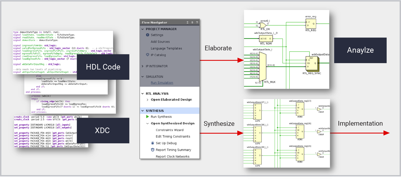
HDL descriptions can be visually reviewed using an elaborated design schematic that cross-probes to the related HDL source code.
Logic synthesis provides control over all aspects of inference and optimization. Assignments can be made:
- Globally using tool and command options
- On specific modules or instances of logical hierarchy using the BLOCK_SYNTH XDC constraint
- On cells and nets using HDL attributes
Types of control include:
- Keeping, flattening, and rebuilding hierarchy
- Inferring or not inferring technology-specific structures
- Selecting the type of dedicated memory resources used for mapping memory arrays
- Assigning the encoding type for Finite State Machines (FSMs)
- Prioritizing performance, utilization, or power
- Applying advanced optimizations such as logical retiming
- Conversion of gated clocks to register enable signals
Vivado logic synthesis supports all levels of customization from pushbutton operation to exploration of different compilation strategies.
Logic synthesis...
- Works with Vivado projects and non-project flows
- Can be run interactively or in batch mode using Tcl
- Runs multiple processes to reduce compile times
- Provides compilation strategies to explore solutions for different design goals
- Supports an incremental compilation mode that reuses data from previous runs to speed up compilation iterations
Design Methodology
When used with Vivado, the UltraFast methodology helps define proper constraints, helps to properly drive the tools and analyze results, and improves overall productivity. The UltraFast Design Methodology is a collection of best hardware design practices accumulated from many years of experience of Vivado experts and their design closure successes on customer designs that push the limits of the tools and technology.

Key Features
UltraFast is documented extensively in User Guides including:
- UG949 - UltraFast Design Methodology Guide for AMD FPGAs and SoCs - an in-depth guide for board and device planning, design and constraint creation, design implementation, and design closure
- UltraFast Design Methodology Quick Reference Guide - a two-page summary of the entire UltraFast Methodology including the most important rules and resolution steps from all ug949 chapters
- UltraFast Design Methodology Timing Closure Quick Reference Guide - a ten-page summary focusing on UltraFast Methodology Timing Closure, including step-by-step procedures for analyzing and resolving all common timing failures and for analyzing and reducing routing congestion.
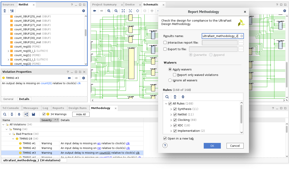
To facilitate compliance with the UltraFast Methodology guidelines, UltraFast Methodology Reports are built into Vivado and generated by default for Vivado projects, providing the benefits of UltraFast without reading a single line of documentation. The Report Methodology feature generates a list of methodology violations found in the current design, broken down by category and severity level for interactive review. Reviewing and addressing the methodology violations ensures designs are given the optimal starting point for implementation, giving the highest chances for successful design closure in the shortest amount of time. Violations that are deemed acceptable can be waived so that they do not reappear in reports.
Providing constraints that are complete and correct is an important part of the UltraFast Methodology. The Timing Constraints Wizard (TCW) analyzes timing constraints and provides step-by-step guidance on supplying missing constraints and fixing invalid constraints. Constraint completeness reduces the chances of hardware bugs resulting from unconstrained timing paths while invalid constraints can misdirect compilation effort toward false timing criticality.
Power constraint quality is critical for accurate power analysis. The Power Constraints Advisor analyzes design switching activity, pinpoints areas that appear to be improperly specified, and generates turnkey XDC power constraints for proper analysis. Vivado power reports also include a confidence level indicating a low, medium, or high quality of power constraint specification, giving feedback on power constraint completeness. A high confidence level ensures the most accurate power analysis, closely matching hardware measurements.
Implementation
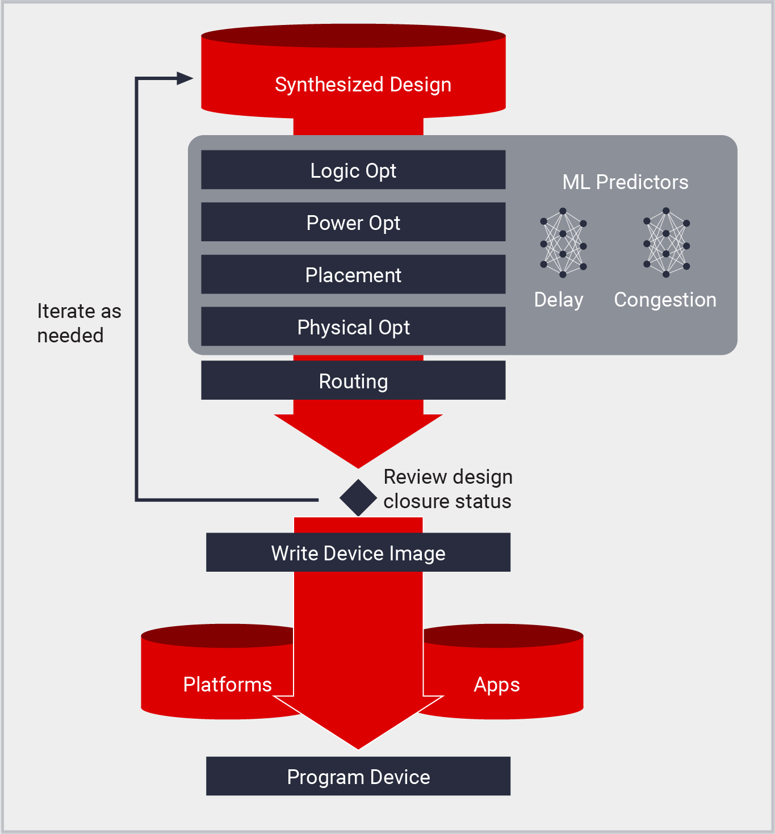
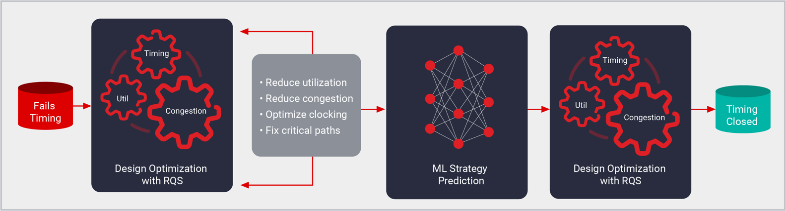
Vivado implementation is the placement and routing tool for AMD devices, generating bitstreams and device images from a synthesized netlist. Implementation enables creation of platforms and custom designs of all sizes from the smallest MPSoCs to the largest monolithic and Stacked Silicon Interconnect Technology (SSIT) devices containing millions of logic cells. Vivado implementation is built on state-of-art partitioning, placement, and routing algorithms guided by Machine Learning-based predictors. Application of ML models allows implementation to achieve higher Quality-of-Results (QoR) in a shorter amount of time with an accurate prediction of routing delays and congestion. Implementation is driven by Xilinx Design Constraints (XDC) to meet design goals for performance, utilization, and power and synthesis works within Vivado Projects and Tcl scripting.
Implementation supports all modes of operation from the pushbutton mode for ease-of-use to sophisticated customized Tcl recipes for handling designs with the toughest performance requirements. Detailed analysis of timing, utilization, power, and other design quality metrics can be performed at any compilation stage: pre-placement, post-placement, and post-routing. The design database can also be saved and restored at any compilation stage using design checkpoint (DCP) files and the design can be visualized and constrained accordingly.

Key Features
Implementation consists of the following processes:
- Logic Optimization: After synthesis, the logical netlist is further optimized at a global level to reduce utilization and reduce logic levels.
- Power Optimization: The design power is reduced using activity gating techniques, with no required intervention and no changes to functionality, and minimal timing impact.
- Placement: Logical netlist cells are placed into physical device resources according to XDC constraints which include timing, floorplan, and manual placement requirements. Placement begins with global resources including IO and clocking resources and logic clusters based on design hierarchy. The global placement phase is followed by the detailed placement and post-placement optimization phases. Placement is guided by ML models that predict routing delays and predict routing congestion which provides greater accuracy and faster compilation compared to traditional statistical methods.
- Routing: Connections between netlist components are assigned to physical device interconnect resources. Similar to placement, routing begins with global resources such as IO and clocking then prioritizes resource assignments according to XDC timing constraints. Final routing phases further optimize routes to meet sign-off setup and hold requirements. Routing congestion is reduced by the use of ML routing congestion prediction during placement.
- Physical Optimization: Physical optimization is a timing-driven process that occurs throughout placement and routing. Unlike logic optimization, physical optimization uses the most accurate timing data available based on placement and routing. Timing impact is evaluated such that only optimization performed results in improved timing. Optimization techniques include replication, retiming, and register re-placement as well as other optimizations specific to the target architecture. Physical optimization can also be run separately after placement and after routing to further improve results.
A design can be analyzed at any compilation stage within implementation. At the center of analysis capabilities are:
- A comprehensive XDC constraint management system allowing modification and verification of timing, power, and physical constraints.
- Report Timing Summary: A powerful static timing analyzer that supports XDC constraints to drive implementation toward specified timing goals. Generates timing reports of critical timing paths, clock interaction, and clock domain crossings (CDCs).
- Report Power: Vectorless propagation supporting XDC switching activity for power analysis. Generates reports to identify areas of higher power consumption.
- Device view: A graphical representation of design placement and routing, along with logical netlist schematics. Enables cross-probing between physical, logical, and source code design views to quickly trace the sources of critical timing paths.
Vivado implementation supports all levels of customization from pushbutton operation to exploration of different compilation strategies and iterative flows for designs with difficult-to-meet requirements.
Implementation...
- Works with Vivado projects and non-project flows
- Can be run interactively or in batch mode using Tcl
- Runs multiple threads to reduce compile times
- Provides compilation strategies to explore solutions for different design goals
- Supports an incremental compilation mode that reuses data from previous runs that can prioritize either compilation speedup or timing closure
Resources

Documentation Portal
Robust online search and navigation of HTML-based technical content.

Design Hubs
Current technical content for specific design tasks, devices, and tools.

Training
Access our library of training materials across a variety of subjects.

Support Community
Expert Support, Design Advisories, Known Issues & Community.